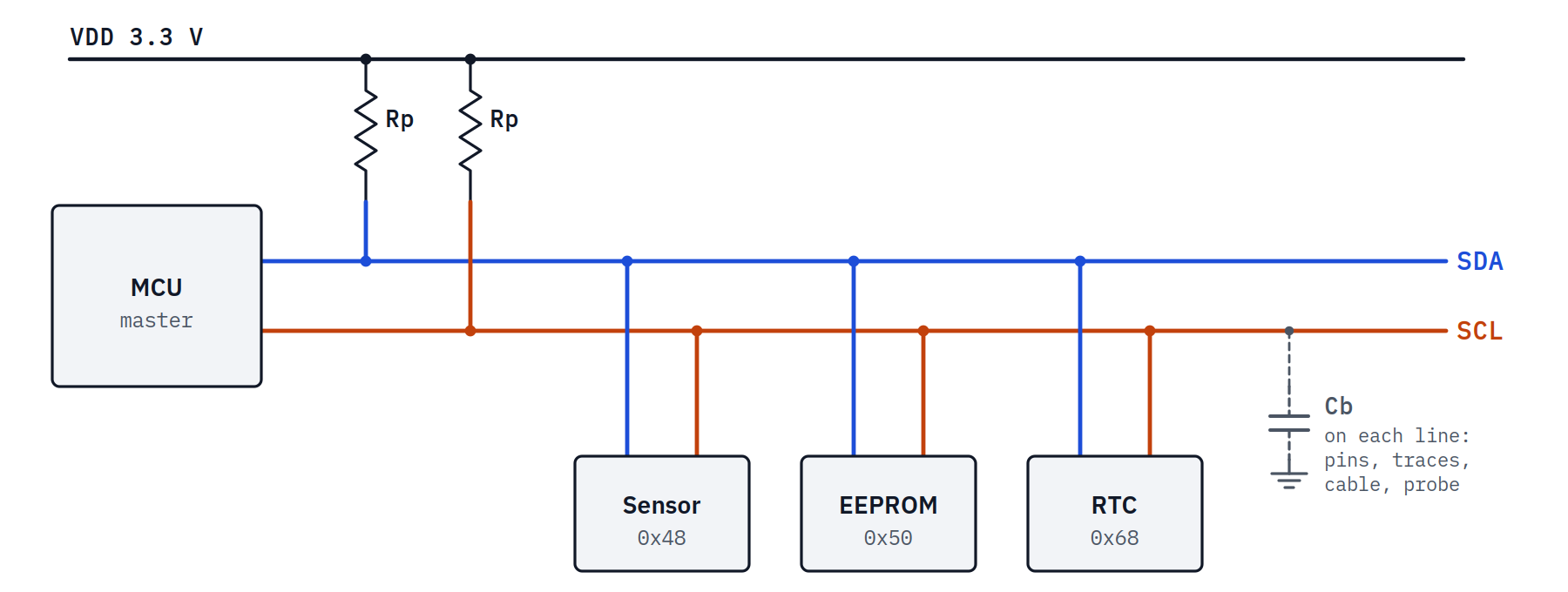
An I²C bus is deceptively simple: two signal wires, common ground, and usually two pull-up resistors. But the resistors are not arbitrary. They determine how quickly SDA and SCL return to HIGH, and how much current a device must sink to pull a line LOW. A 4.7 kΩ pair works on countless hobby boards, which is exactly why it gets copied into designs where it does not.
Why I²C uses pull-ups
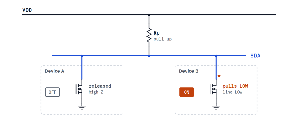
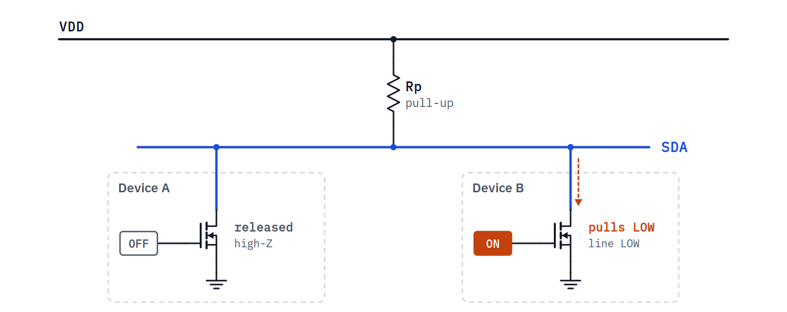
I²C devices use open-drain (or open-collector) outputs. A device can actively pull a line LOW, but it never drives it HIGH. When every device releases the line, the pull-up resistor pulls it toward the bus supply voltage. That is what lets many devices share two wires: no output can fight another, and the bus behaves as a wired-AND, which I²C uses for clock synchronisation and multi-master arbitration.
Every pin, trace, connector and cable on the bus adds capacitance. Together they form the bus capacitance Cb, and every rising edge is that capacitance charging through the pull-up. More capacitance means a slower rise for the same resistor. The specification allows up to 10 pF per device pin; traces and cables add their own share, and a long ribbon cable or an oscilloscope probe can easily become the largest part of it.
What the bus does during a transfer
Before sizing anything, it helps to see where the rising edges come from. A transfer starts with a START condition: SDA falls while SCL is HIGH. The master then clocks out a 7-bit address and a read/write bit, and the addressed device answers by pulling SDA LOW during the ninth clock pulse (ACK). Data bytes follow in the same rhythm, each acknowledged by the receiver, and a STOP condition, SDA rising while SCL is HIGH, ends the transfer. SDA may only change while SCL is LOW; a change while SCL is HIGH is, by definition, a START or a STOP.
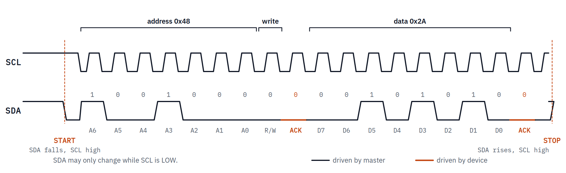
Every rising edge in that diagram, on both lines, is produced by a pull-up resistor charging Cb. No device drives the line HIGH. If those edges are too slow, a receiver can sample a bit before the line has crossed its HIGH threshold.
Estimate the upper resistance limit
For a first-order approximation, the rise time measured from 30 % to 70 % of the supply is:
tr ≈ 0.8473 × Rp × Cb
The factor 0.8473 is ln(0.7 / 0.3), the time an RC circuit needs to charge from 30 % to 70 % of its final value. Those two levels are the standard I²C input thresholds, VIL = 0.3 × VDD and VIH = 0.7 × VDD. Here Rp is the pull-up resistance in ohms and Cb the total bus capacitance in farads. Rearranging gives:
Rp(max) ≈ tr(max) / (0.8473 × Cb)
The NXP I²C-bus specification, UM10204, sets these limits per speed mode, measured under its defined conditions:
| Mode | Clock | Max rise time | Max bus capacitance | Min sink current at VOL 0.4 V |
|---|---|---|---|---|
| Standard-mode | 100 kHz | 1000 ns | 400 pF | 3 mA |
| Fast-mode | 400 kHz | 300 ns | 400 pF | 3 mA |
| Fast-mode Plus | 1 MHz | 120 ns | 550 pF | 20 mA |
Consider a 3.3 V bus with 200 pF of estimated bus capacitance:
| Pull-up | 30–70 % rise time | Standard-mode (1000 ns) | Fast-mode (300 ns) |
|---|---|---|---|
| 10 kΩ | 1.69 µs | too slow | too slow |
| 4.7 kΩ | 0.80 µs | fits | too slow |
| 2.2 kΩ | 0.37 µs | fits | too slow |
| 1.5 kΩ | 0.25 µs | fits | fits |
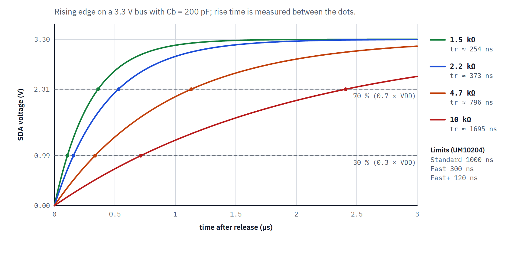
The waveform at the top of this article shows what that means at 400 kHz: with 4.7 kΩ the clock barely crosses the 70 % threshold before it is pulled LOW again, leaving almost no valid HIGH time. With 1.5 kΩ the edges are clean.
The table is not an approval of 1.5 kΩ for every device. The lower resistance limit matters too.
Check the LOW-state current
A device holding a line LOW must sink the pull-up current, roughly I ≈ (VDD − VOL) / Rp. For Standard- and Fast-mode, the specification requires devices to sink at least 3 mA while keeping VOL at or below 0.4 V, which gives the lower limit:
Rp(min) ≈ (VDD − VOL(max)) / IOL
On a 3.3 V bus that is (3.3 − 0.4) V / 3 mA ≈ 967 Ω; on a 5 V bus about 1.53 kΩ. At 3.3 V with a 1.5 kΩ resistor, the current is approximately 1.93 mA, comfortably inside the limit. Still check each datasheet’s allowed LOW-output current and voltage rather than assuming every sensor has identical drive capability.
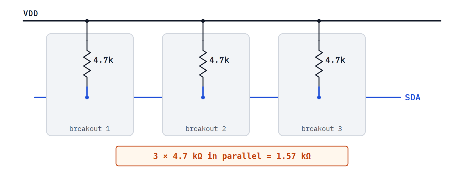
Remember that pull-ups can exist on several breakout boards at once. Three modules, each with a 4.7 kΩ pull-up on the same line, create an effective resistance of roughly 1.57 kΩ. Pull-ups in parallel do not remain 4.7 kΩ, and with enough modules the total can drop below Rp(min). Remove or disconnect the extras; some breakouts have a solder jumper for exactly this.
The design window
Put both limits together and every speed mode gets a window: above Rp(min), below Rp(max). For a 3.3 V bus with devices that sink 3 mA:
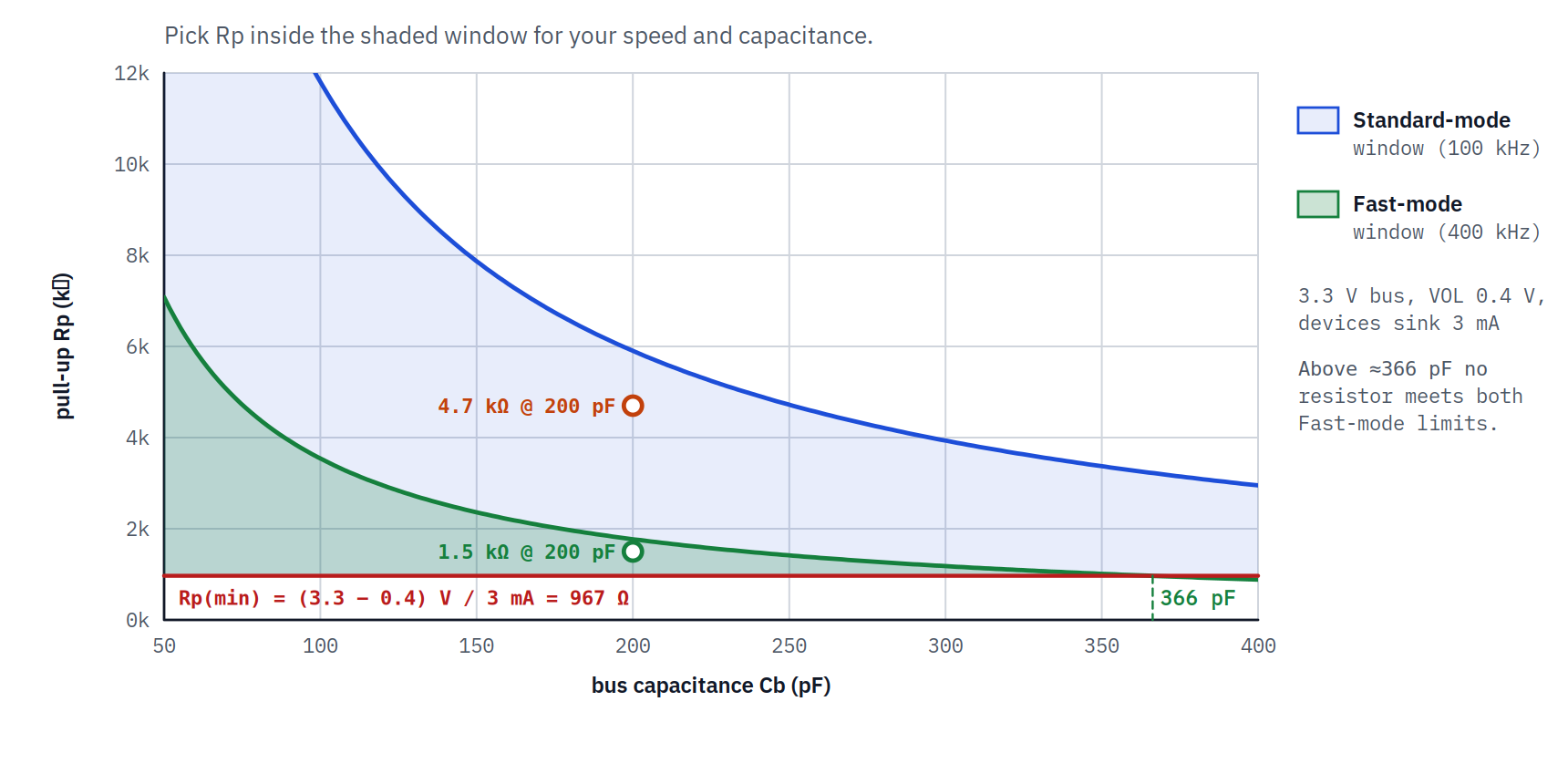
At 200 pF, Standard-mode leaves a wide choice between about 1 kΩ and 5.9 kΩ, so 4.7 kΩ is fine there. Fast-mode narrows the window to about 1 kΩ to 1.8 kΩ. Above roughly 366 pF, no single resistor meets both Fast-mode limits: reduce the capacitance, lower the clock speed, or add a bus buffer or a rise-time accelerator such as the LTC4311.
Within the window, stay clear of both edges. A value nearer Rp(max) saves power; a value nearer Rp(min) gives faster edges and better noise immunity.
Voltage domains matter
Do not pull a 3.3 V-only signal pin up to 5 V unless it is explicitly rated for that voltage. A common ground is required, but sharing ground alone does not make mixed-voltage signals compatible. Where two domains meet, use a bidirectional level shifter. The classic discrete version uses one N-channel MOSFET per line, with a pull-up on each side:
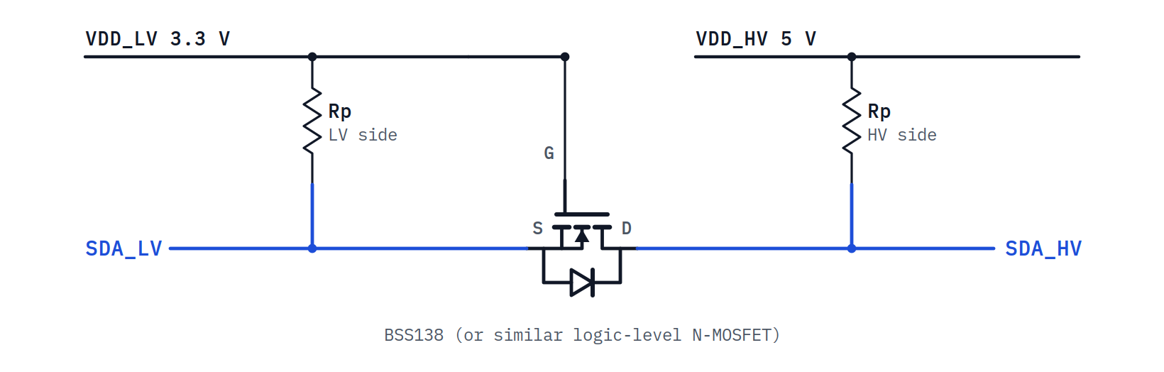
When the 3.3 V side pulls LOW, the MOSFET’s gate-source voltage rises and it conducts, pulling the 5 V side LOW as well. When the 5 V side pulls LOW, the body diode first drags the 3.3 V side down until the MOSFET turns on. When nobody pulls, each side rises to its own supply through its own pull-up. Size those pull-ups for each side’s own capacitance. Dedicated translators such as the PCA9306 do the same job in one package; for long cables or heavy loads, use a bus buffer designed for the speeds, voltages and capacitances involved.
Practical debugging steps
- Check the bus voltage and pull-up arrangement with power OFF before connecting a questionable module. Measuring from SDA and SCL to VDD shows the combined pull-up value, including any hidden ones on breakouts.
- Measure idle SDA and SCL; both should be HIGH when the bus is free.
- Inspect rise time on an oscilloscope at the farthest device, not only next to the master. The probe adds capacitance too.
- Reduce clock speed to see whether timing margin is the issue.
- Check for missing grounds, duplicate addresses and unusually long or noisy cables.
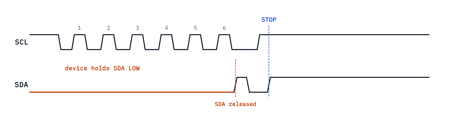
- If a device holds SDA LOW continuously, treat bus recovery as a separate problem from pull-up sizing.
A stuck SDA usually means a device was interrupted in the middle of a byte, for example by an MCU reset, and is still waiting for clock pulses to finish it. The specification’s bus clear procedure handles this: the master clocks SCL, up to nine pulses, until the device releases SDA, and then sends a STOP. If the line stays LOW after nine pulses, the device needs a hardware reset or a power cycle.
A 4.7 kΩ pair can be an excellent starting point for a short, lightly loaded 100 kHz bus. The correct production value, however, comes from the device specifications, the total capacitance and an actual measurement.